DOWNLOAD
Part No. | Input | Output | Burst- Mode | Interface | Temp. | Fiber |
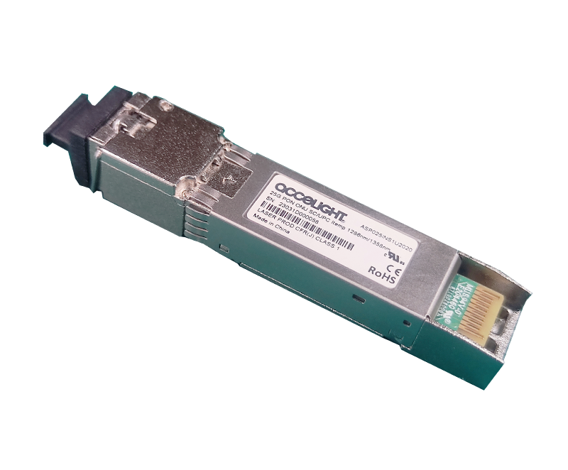
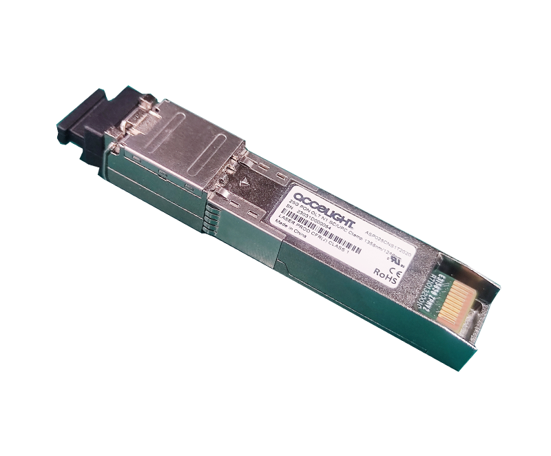
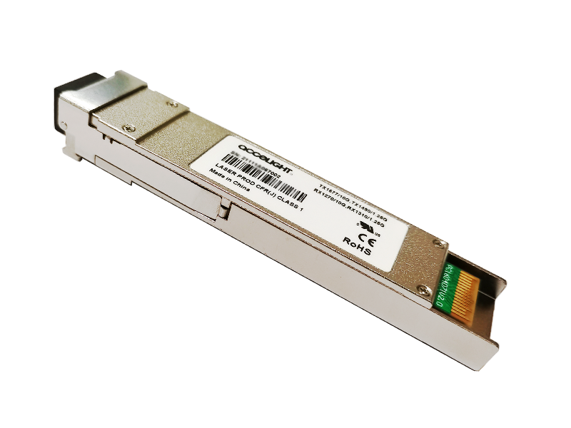
ASP-PR-GU-20 | AC | AC | LVTTL | SC | Industrial | SMF |
Functional Diagram

Absolute Maximum Ratings
Parameter | Symbol | Min. | Max. | Unit |
Storage Temperature | Ts | -40 | 85 | °C |
Supply Voltage | Vcc | -0.5 | 4.0 | V |
Operating Relative Humidity | RH | 5 | 95 | % |
Recommended Operating Conditions
Parameter | Symbol | Min. | Typical | Max. | Unit |
Operating Case Temperature | Tc | -40 | 85 | °C | |
Power Supply Voltage | Vcc | 3.15 | 3.3 | 3.45 | V |
Power Supply Current | Icc | 450 | mA | ||
Data Rate | 9.95328 | Gbps |
Optical Characteristics
Parameter | Symbol | Min. | Typical | Max. | Unit |
Data rate | 9.95328 | Gbps | |||
Transmitter | |||||
Centre Wavelength | λC | 1260 | 1270 | 1280 | nm |
Spectral Width (-20dB) | Δλ | 1 | nm | ||
Side Mode Suppression Ratio | SMSR | 30 | dB | ||
Average Output Power | Pout | +4 | +9 | dBm | |
Extinction Ratio | ER | 6 | dB | ||
Rise/Fall Time(with-out filter) | tr/tf | 38 | ps | ||
Output Optical Eye | ITU-T G.9807.1 Compliant | ||||
Optical Output Power with TX OFF | P_off | -45 | dBm | ||
Receiver | |||||
Centre Wavelength | λc | 1575 | 1580 | nm | |
Receiver Sensitivity | Pmin | -28 | dBm | ||
Overload Optical Power | Pmax | -8 | dBm | ||
LOS De-Assert | LOSD | -29 | dBm | ||
LOS Assert | LOSA | -42 | dBm | ||
LOS Hysteresis | 0.5 | 6 | dB | ||
RSSI resolution @ Full temperature range | -3 | +3 | dB | ||
WDM Filter ISO | ISO(1560) | 35 | dB | ||
ISO(1600) | 35 | dB | |||


Electrical Characteristics
Parameter | Symbol | Min. | Typ. | Max | Unit | Notes |
Transmitter | ||||||
CML Input(Differential) | Vin | 200 | 1000 | mVpp | ||
Input Impedance (Differential) | Zin | 85 | 100 | 115 | ohm | |
Tx_Burst_Enable Input Voltage | H | 2 | Vcc | V | ||
L | 0 | 0.8 | V | |||
Tx_FAULT Output Voltage | H | 2.4 | Vcc+0.3 | V | ||
L | 0 | 0.4 | V | |||
Tx_SD Output Voltage | H | 2.4 | Vcc+0.3 | V | Laser on indicator | |
L | 0 | 0.4 | V | Laser off indicator | ||
Receiver | ||||||
CML Output(Differential) | Vout | 340 | 900 | mVpp | AC coupled outputs | |
Output Impedance (Differential) | Zout | 80 | 100 | 120 | ohm | |
Rx Los output Voltage | H | 2.4 | Vcc+0.3 | V | ||
L | 0 | 0.4 | V | |||
Rx Los Assert time | Tassert | - | 100 | us | ||
Rx Los De-Assert time | TDe-assert | - | 100 | us | ||
SFP+ Transceiver Electrical Pad Layout


Pin Descriptions
Pin | Name | Function | Plug Seq. |
1 | VeeT | Transmitter Ground | 1 |
2 | TX Fault | Transmitter Fault Indication | 3 |
3 | TX_Burst_Enable | Burst Enable | 3 |
4 | SDA | Module Definition 2 | 3 |
5 | SCL | Module Definition 1 | 3 |
6 | MOD-ABS | Module Definition 0 | 3 |
7 | TX_SD | TX signal detector (LVTTL) | 3 |
8 | RX_LOS | Loss of Signal | 3 |
9 | P_Down | Power down (LVTTL) | 3 |
10 | VeeR | Receiver Ground | 1 |
11 | VeeR | Receiver Ground | 1 |
12 | RD- | Inv. Received Data Out | 3 |
13 | RD+ | Received Data Out | 3 |
14 | VeeR | Receiver Ground | 1 |
15 | VccR | Receiver Power | 2 |
16 | VccT | Transmitter Power | 2 |
17 | VeeT | Transmitter Ground | 1 |
18 | TD+ | Transmit Data In | 3 |
19 | TD- | Inv. Transmit Data In | 3 |
20 | VeeT | Transmitter Ground | 1 |
EEPROM
The serial interface uses the 2-wire serial CMOS EEPROM protocol defined for the ATMEL AT24C02/04 family of components. When the serial protocol is activated, the host generates the serial clock signal (SCL). The positive edge clocks data into those segments of the EEPROM that are not writing protected within the SFP+ transceiver. The negative edge clocks data from the SFP+ transceiver. The serial data signal (SDA) is bi-directional for serial data transfer. The host uses SDA in conjunction with SCL to mark the start and end of serial protocol activation. The memories are organized as a series of 8-bit data words that can be addressed individually or sequentially.
The Module provides diagnostic information about the present operating conditions. The transceiver generates this diagnostic data by digitization of internal analog signals. Calibration and alarm/warning threshold data is written during device manufacture. Received power monitoring, transmitted power monitoring, bias current monitoring, supply voltage monitoring and temperature monitoring all are implemented. If the module is defined as external calibrated, the diagnostic data are raw A/D values and must be converted to real world units using calibration constants stored in EEPROM locations 56 – 95 at wire serial bus address A2h. The digital diagnostic memory map specific data field define as following .For detail EEPROM information, please refer to the related document of SFF 8472 Rev 10.2.

Digital Diagnostic Monitor Specification
Address | Parameter | Range | NOTES |
96-97 | Temperature | -40 to 90°C | Case Temperature |
98-99 | Vcc Voltage | 0V to 6.55V | |
100-101 | Bias Current | 0 to 131mA | Unit 2 uA |
102-103 | TX Power | -10 to 8.2 dBm | Unit 0.2uW |
104-105 | RX Power | -30 to -8 dBm | Unit 0.1uW |
Recommend Circuit Schematic


Copyright 2022 ATI. All rights reserved.
Copyright 2022 ATI. All rights reserved.
Please fill the following information, we can better provide our services.