DOWNLOAD
Part No. | Data Rate | AOC Length | Temp. | DDMI |
AQP040CH1010xxx | 40Gbps | 1m-100m | 0~+70℃ | Yes |
AQP040CH2010xxx | 40Gbps | 1m-100m | 0~+70℃ | Yes |
AQP040CH4010xxx | 40Gbps | 1m-100m | 0~+70℃ | Yes |
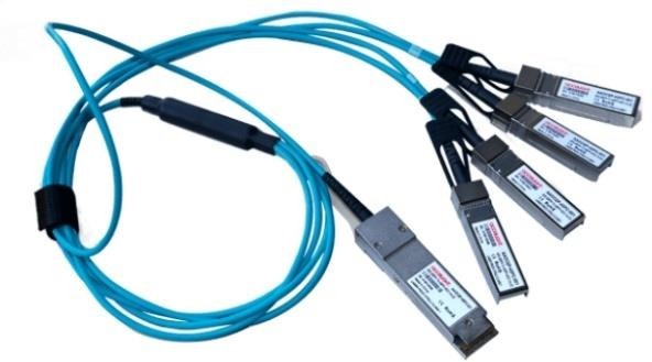
Note1: H1= QSFP+ to 4*SFP+ AOC, both side unfixed; H2= QSFP+ to 4*SFP+ AOC, both side fixed; H4= QSFP+ to 4*SFP+ AOC, SFP+ side unfixed, QSFP+ side fixed.
Note2: Length measured OM3 fiber. xxx denotes the AOC length with unit meter. For example, 001 denotes 1m, 002
denote 2m …
Absolute Maximum Ratings
Parameter | Symbol | Min. | Max. | Unit |
Storage Temperature | Ts | -40 | 85 | °C |
Supply Voltage | Vcc | -0.5 | 3.6 | V |
Operating Relative Humidity | RH | 5 | 85 | % |
Recommended Operating Conditions
Parameter | Symbol | Min. | Typical | Max. | Unit |
Operating Case Temperature | Tc | 0 | 70 | °C | |
Power Supply Voltage | Vcc | 3.135 | 3.3 | 3.465 | V |
QSFP+ Aggregate Bit Rate | BRAVE | 41.25 | Gbps | ||
SFP+ Bit Rate | BRLANE | 10.3125 | Gbps |
QSFP+ Transceiver Electrical Pad Layout

Pin Arrangement and Definition
Pin | Logic | Symbol | Description | Plug Sequence | Notes |
1 | GND | Ground | 1 | 1 | |
2 | CML-I | Tx2n | Transmitter Inverted Data Input | 3 | |
3 | CML-I | Tx2p | Transmitter Non- Inverted Data Input | 3 | |
4 | GND | Ground | 1 | 1 | |
5 | CML-I | Tx4n | Transmitter Inverted Data | 3 | |
Input | |||||
6 | CML-I | Tx4p | Transmitter Non- Inverted Data Input | 3 | |
7 | GND | Ground | 1 | 1 | |
8 | LVTTL-I | ModSelL | Module Select | 3 | |
9 | LVTTL-I | ResetL | Module Reset | 3 | |
10 | VccRx | +3.3V Power Supply Receiver | 2 | 2 | |
11 | LVCMOS- I/O | SCL | 2-wire serial interface clock | 3 | |
12 | LVCMOS- I/O | SDA | 2-wire serial interface data | 3 | |
13 | GND | Ground | 1 | 1 | |
14 | CML-O | Rx3p | Receiver Non- Inverted Data Output | 3 | |
15 | CML-O | Rx3n | Receiver Inverted Data Output | 3 | |
16 | GND | Ground | 1 | 1 | |
17 | CML-O | Rx1p | Receiver Non- Inverted Data Output | 3 | |
18 | CML-O | Rx1n | Receiver Inverted Data Output | 3 | |
19 | GND | Ground | 1 | 1 | |
20 | GND | Ground | 1 | 1 | |
21 | CML-O | Rx2n | Receiver Inverted Data Output | 3 | |
22 | CML-O | Rx2p | Receiver Non- Inverted Data Output | 3 | |
23 | GND | Ground | 1 | 1 | |
24 | CML-O | Rx4n | Receiver Inverted Data Output | 3 | |
25 | CML-O | Rx4p | Receiver Non- Inverted Data Output | 3 | |
26 | GND | Ground | 1 | 1 | |
27 | LVTTL-O | ModPrsL | Module Present | 3 | |
28 | LVTTL-O | IntL/RxLOSL | Interrupt.OptionallyConfigurable As RxLOSL Via The Management Interface (SFF- | 3 | |
8636). | |||||
29 | VccTx | +3.3V Power supply transmitter | 2 | 2 | |
30 | Vcc1 | +3.3V Power supply | 2 | 2 | |
31 | LVTTL-I | LPMode/TxDis | Low Power Mode. | 3 | |
OptionallyConfigurable As TxDis Via The ManagementInterface (SFF- | |||||
8636). | |||||
32 | GND | Ground | 1 | 1 | |
33 | CML-I | Tx3p | Transmitter Non- Inverted Data Input | 3 | |
34 | CML-I | Tx3n | TransmitterInverted Data Input | 3 | |
35 | GND | Ground | 1 | 1 | |
36 | CML-I | Tx1p | Transmitter Non-Inverted Data Input | 3 | |
37 | CML-I | Tx1n | Transmitter Inverted Data Input | 3 | |
38 | GND | Ground | 1 | 1 |
1: GND is the symbol for signal and supply (power) common for the QSFP+ module. All are common within the QSFP+ module and all module voltages are referenced to this potential unless otherwise noted. Connect thesedirectly to the host board signal-common ground plane. |
2: Vcc Rx, Vcc1 and Vcc Tx are the receiver and transmitter power supplies and shall be applied concurrently. Vcc Rx Vcc1 and Vcc Tx may be internally connected within the QSFP+ Module in any combination. Theconnector pins are each rated for a maximum current of 500mA. |
SFP+ Transceiver Electrical Pad Layout

Pin Arrangement and Definition
Pin |
Name |
Function | Plug Seq. |
Notes |
1 | VeeT | Transmitter Ground | 1 | Note 5 |
2 |
TX Fault | Transmitter Fault Indication |
3 |
Note 1 |
3 | TX Disable |
Transmitter Disable |
3 | Note 2, Module disables on high or open |
4 | SDA | Module Definition 2 | 3 | Data line for Serial ID. |
5 | SCL | Module Definition 1 | 3 | Clock line for Serial ID. |
6 | MOD-ABS | Module Definition 0 | 3 | Note 3 |
7 |
RS0 |
RX Rate Select (LVTTL). |
3 | This pin has an internal 30k pull down to ground. A signal on this pin will not affect module performance. |
8 | LOS | Loss of Signal | 3 | Note 4 |
9 |
RS1 |
TX Rate Select (LVTTL). |
1 | This pin has an internal 30k pull down to ground. A signal on this pin will not affect module performance. |
10 | VeeR | Receiver Ground | 1 | Note 5 |
11 | VeeR | Receiver Ground | 1 | Note 5 |
12 | RD- | Inv. Received Data Out | 3 | Note 6 |
13 | RD+ | Received Data Out | 3 | Note 6 |
14 | VeeR | Receiver Ground | 1 | Note 5 |
15 | VccR | Receiver Power | 2 | 3.3V ± 5%, Note 7 |
16 | VccT | Transmitter Power | 2 | 3.3V ± 5%, Note 7 |
17 | VeeT | Transmitter Ground | 1 | Note 5 |
18 | TD+ | Transmit Data In | 3 | Note 8 |
19 | TD- | Inv. Transmit Data In | 3 | Note 8 |
20 | VeeT | Transmitter Ground | 1 | Note 5 |
1) TX Fault is an open collector/drain output, which should be pulled up with a 4.7K – 10KΩ resistor on the host board. Pull up voltage between 2.0V and VccT/R+0.3V. When high, output indicates a laser fault of some kind. Low indicates normal operation. In the low state, the output will be pulled to < 0.8V.
2) TX disable is an input that is used to shut down the transmitter optical output. It is pulled up within the module with a 4.7K~10 K Ω resistor. Its states are:
Low (0 – 0.8V): Transmitter on (>0.8, < 2.0V): Undefined
High (2.0 – 3.465V): Transmitter Disabled Open: Transmitter Disabled
3) Module Absent, connected to VeeT or VeeR in the module.
4) LOS (Loss of Signal) is an open collector/drain output, which should be pulled up with a 4.7K – 10KΩ resistor on host board. Pull up voltage between 2.0V and VccT/R+0.3V. When high, this output indicates the received optical power is below the worst-case receiver sensitivity (as defined by the standard in use). Low indicates normal operation. In the low state, the output will be pulled to < 0.8V.
5) VeeR and VeeT may be internally connected within the SFP+ module.
6) RD-/+: These are the differential receiver outputs. They are AC coupled 100Ω differential lines which should be terminated with 100Ω (differential) at the user SERDES. The AC coupling is done inside the module and is thus not required on the host board. The voltage swing on these lines will be between 370 and 700 mV differential (185 –350mV single ended) when properly terminated.
7) VccR and VccT are the receiver and transmitter power supplies. They are defined as 3.3V±5% at the SFP+ connector pin. Maximum supply current is 430mA. Recommended host board power supply filtering is shown below. Inductors with DC resistance of less than 1 ohm should be used in order to maintain the required voltage at the SFP+ input pin with 3.3V supply voltage. When the recommended supply-filtering network is used, hot plugging of the SFP+ transceiver module will result in an inrush current of no more than 30mA greater than the steady state value. VccR and VccT may be internally connected within the SFP+ transceiver module.
8) TD-/+: These are the differential transmitter inputs. They are AC-coupled, differential lines with 100Ω differential termination inside the module. The AC coupling is done inside the module and is thus not required on the host board.

Copyright 2022 ATI. All rights reserved.
Copyright 2022 ATI. All rights reserved.
Please fill the following information, we can better provide our services.