DOWNLOAD
Part number | Description |
AAQSSP040Cxxx | XXX=different cable lengths on OM3 Multimode Fiber (MMF)-Note |
Xxx | cable lengths on OM3 Multimode Fiber (MMF) |
003 | 3m |
005 | 5m |
007 | 7m |
010 | 10m |
050 | 50m |
100 | 100m |
Note:
1. Cable length’s range of SFP+ end to 1- 4 point must be 0.5 to 3 m.
2. More detail product selection and cable lengths,please contact sales
Absolute Maximum Ratings
Parameter | Symbol | Min. | Typ. | Max. | Unit | Note |
Storage Temperature | Ts | -40 | - | 85 | ºC | |
Relative Humidity | RH | 5 | - | 95 | % | |
Power Supply Voltage | VCC | -0.3 | - | 4 | V | |
Signal Input Voltage | Vcc-0.3 | - | Vcc+0.3 | V |
Recommended Operating Conditions
Parameter | Symbol | Min. | Typ. | Max. | Unit | Note |
Case Operating Temperature | Tcase | 0 | - | 70 | ºC | Without air flow |
Power Supply Voltage | VCC | 3.14 | 3.3 | 3.46 | V | |
Power Supply Current |
ICC | 300 | mA | Per cable end- SFP+ | ||
- | 450 | mA | Per cable end- QSFP+ | |||
Data Rate | BR | 10.3125 | Gbps | SFP+ Bit rate | ||
41.25 | Gbps | QSFP+ Bit rate |
Pin Assignment

Pin | Symbol | Name/Description | NOTE |
1 | VEET | Transmitter Ground (Common with Receiver Ground) | 1 |
2 | TFAULT | Transmitter Fault. | 2 |
3 | TDIS | Transmitter Disable. Laser output disabled on high or open. | 3 |
4 | SDA | 2-wire Serial Interface Data Line | 4 |
5 | SCL | 2-wire Serial Interface Clock Line | 4 |
6 | MOD_ABS | Module Absent. Grounded within the module | 4 |
7 | RS0 | Rate Select 0 | 5 |
8 | LOS | Loss of Signal indication. Logic 0 indicates normal operation. | 6 |
9 | RS1 | No connection required | 1 |
10 | VEER | Receiver Ground (Common with Transmitter Ground) | 1 |
11 | VEER | Receiver Ground (Common with Transmitter Ground) | 1 |
12 | RD- | Receiver Inverted DATA out. AC Coupled | |
13 | RD+ | Receiver Non-inverted DATA out. AC Coupled | |
14 | VEER | Receiver Ground (Common with Transmitter Ground) | 1 |
15 | VCCR | Receiver Power Supply | |
16 | VCCT | Transmitter Power Supply | |
17 | VEET | Transmitter Ground (Common with Receiver Ground) | 1 |
18 | TD+ | Transmitter Non-Inverted DATA in. AC Coupled. | |
19 | TD- | Transmitter Inverted DATA in. AC Coupled. | |
20 | VEET | Transmitter Ground (Common with Receiver Ground) | 1 |
Notes:
Circuit ground is internally isolated from chassis ground.
TFAULT is an open collector/drain output, which should be pulled up with a 4.7k – 10k Ohms resistor on the host board if intended for use. Pull up voltage should be between 2.0V to Vcc + 0.3V.A high output indicates a transmitter fault caused by either the TX bias current or the TX output power exceeding the preset alarm thresholds. A low output indicates normal operation. In the low state, the output is pulled to <0.8V.
3. Laser output disabled on TDIS >2.0V or open, enabled on TDIS <0.8V.
4. Should be pulled up with 4.7kΩ- 10kΩ host board to a voltage between 2.0V and 3.6V. MOD_ABS pulls line low to indicate module is plugged in.
5. Internally pulled down per SFF-8431 Rev 4.1.
6.LOS is open collector output. It should be pulled up with 4.7kΩ – 10kΩ on host board to a voltage between 2.0V and 3.6V. Logic 0 indicates normal operation; logic 1 indicates loss of signal.

Pin | Symbol | Name/Description | NOTE |
1 | GND | Transmitter Ground (Common with Receiver Ground) | 1 |
2 | Tx2n | Transmitter Inverted Data Input | |
3 | Tx2p | Transmitter Non-Inverted Data output | |
4 | GND | Transmitter Ground (Common with Receiver Ground) | 1 |
5 | Tx4n | Transmitter Inverted Data Input | |
6 | Tx4p | Transmitter Non-Inverted Data output | |
7 | GND | Transmitter Ground (Common with Receiver Ground) | 1 |
8 | ModSelL | Module Select | |
9 | ResetL | Module Reset | |
10 | VccRx | 3.3V Power Supply Receiver | 2 |
11 | SCL | 2-Wire serial Interface Clock | |
12 | SDA | 2-Wire serial Interface Data | |
13 | GND | Transmitter Ground (Common with Receiver Ground) | |
14 | Rx3p | Receiver Non-Inverted Data Output | |
15 | Rx3n | Receiver Inverted Data Output | |
16 | GND | Transmitter Ground (Common with Receiver Ground) | 1 |
17 | Rx1p | Receiver Non-Inverted Data Output | |
18 | Rx1n | Receiver Inverted Data Output | |
19 | GND | Transmitter Ground (Common with Receiver Ground) | 1 |
20 | GND | Transmitter Ground (Common with Receiver Ground) | 1 |
21 | Rx2n | Receiver Inverted Data Output | |
22 | Rx2p | Receiver Non-Inverted Data Output | |
23 | GND | Transmitter Ground (Common with Receiver Ground) | 1 |
24 | Rx4n | Receiver Inverted Data Output | 1 |
25 | Rx4p | Receiver Non-Inverted Data Output | |
26 | GND | Transmitter Ground (Common with Receiver Ground) | 1 |
27 | ModPrsl | Module Present | |
28 | IntL | Interrupt | |
29 | VccTx | 3.3V power supply transmitter | 2 |
30 | Vcc1 | 3.3V power supply | 2 |
31 | LPMode | Low Power Mode,not connect | |
32 | GND | Transmitter Ground (Common with Receiver Ground) | 1 |
33 | Tx3p | Transmitter Non-Inverted Data Input | |
34 | Tx3n | Transmitter Inverted Data Output | |
35 | GND | Transmitter Ground (Common with Receiver Ground) | 1 |
36 | Tx1p | Transmitter Non-Inverted Data Input | |
37 | Tx1n | Transmitter Inverted Data Output | |
38 | GND | Transmitter Ground (Common with Receiver Ground) | 1 |
Notes:
1. GND is the symbol for signal and supply (power) common for QSFP+ modules. All are common within the QSFP+ module and all module voltages are referenced to this potential unless otherwise noted. Connect these directly to the host board signal common ground plane.
2. VccRx, Vcc1 and VccTx are the receiving and transmission power suppliers and shall be applied concurrently. Recommended host board power supply filtering is shown below. Vcc Rx, Vcc1 and Vcc Tx may be internally connected within the QSFP+ transceiver module in any combination. The connector pins are each rated for a maximum current of 500mA.
Host - Transceiver Interface Block Diagram

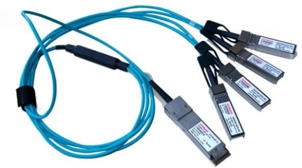
Cable END—SFP+

Cable END—QSFP+
Copyright 2022 ATI. All rights reserved.
Copyright 2022 ATI. All rights reserved.
Please fill the following information, we can better provide our services.