DOWNLOAD
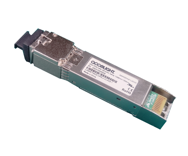
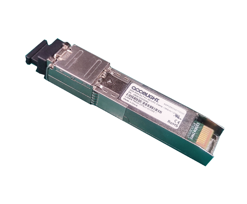
Part No. | Input | Output | Interface | Temp. | Fiber |
ASP-PR-GT-DC-30 | AC/10G | DC/10G/2.5G | SC | Standard | SMF |
Note: Interface provide APC/UPC to choose.
Absolute Maximum Ratings
Parameter | Symbol | Min. | Max. | Unit |
Storage Temperature | Ts | -40 | 85 | °C |
Supply Voltage | Vcc | -0.5 | 3.6 | V |
Operating Relative Humidity | RH | 5 | 95 | % |
Recommended Operating Conditions
Parameter | Symbol | Min. | Typical | Max. | Unit |
Operating Case Temperature | Tc | 0 | 70 | °C | |
Power Supply Voltage | Vcc | 3.15 | 3.3 | 3.45 | V |
Power Supply Current | Icc | 750 | mA | ||
Relative Humidity | RH | 5 | 85 | % | |
Data rate | TX_side | 9.95328 | Gbps | ||
Rx_side | 9.95328/2.48832 |
10G Transmitter Electrical and Optical Characteristics
Parameter | Symbol | Min. | Typ. | Max | Unit | Notes | |
Electrical | |||||||
CML Input(Differential) | Vin | 100 | 850 | mVpp | |||
Input Impedance (Differential) | Zin | 85 | 100 | 115 | ohm | ||
Tx_Disable | Disable | 2 | Vcc | V | |||
Tx_Enable | Enable | GND | GND+0.8 | V | |||
TX_FAULT | FAULT | 2.4 | Vcc | V | |||
TX_FAULT | Normal | GND | GND+0.4 | V | |||
Optical | |||||||
Data Rate | @Tx | 9.95328 | Gbps | ||||
The type of optical | EML laser | ||||||
Centre Wavelength Spectral Width (-20dB) | λC | 1575 | 1577 | 1580 | nm | ||
∆λ | 1 | nm | |||||
Average Output Power(N1) | EOL | Pout | +2 | +5 | dBm | ||
Side Mode Suppression Mode | SMSR | 30 | dB | ||||
Extinction Ratio | ER | 8.2 | dB | Note3 | |||
Transmitter tolerance to reflected power | CW | -15 | dB | ||||
Optical Output Power with Tx OFF | P_off | -39 | dBm | ||||
Output Optical Eye | ITU-T G.9807.1 Compliant | ||||||
10G Receiver Electrical and Optical Characteristics
Parameter | Symbol | Min. | Typical | Max. | Unit | |
Electrical | ||||||
LVCML | Vout | 300 | 800 | mV | ||
Outputs(Differential) | ||||||
Output Impedance (Differential) | Zout | 85 | 100 | 115 | ohm | |
Rx_SD | High Low | 2 | Vcc | V | ||
0 | 0.8 | V | ||||
Optical | ||||||
Data Rate | @Rx | 9.953/2.488 | Gbps | |||
Centre Wavelength | λC | 1260 | 1270 | 1280 | nm | |
SD Hysteresis | 0.5 | dB | ||||
XGS-PON Sensitivity(N1) | @9.95G BER=1E-3 | -26 | dBm | |||
@2.488G BER=1E-4 | dBm | |||||
XGS-PON | @9.95G | -5 | -27.5 | dBm | ||
@2.488G | -7 | dBm | ||||
Receiver Reflectance | dB | |||||
PDL | -12 | dB | ||||
Consecutive Identical Digit Immunity | 72 | 0.5 | bit | |||
Rx_SD | Assert | -40 |
| |||
De-assert | -29 | |||||
Pin Functions
Pin | Name | Function | Plug Seq. |
1 | NC | 1st | |
2 |
Tx_Fault | TX Fault is an open collector/drain output, which should be pulled up with a 4.7K – 10KΩ resistor on thehost board. When high, output indicates a laser fault of some kind. Low indicates normal operation. |
3rd |
3 |
Tx_Disable | Tx Disable. LVTTL input. Laser output is disabled when this pin is asserted high or left unconnected. Laser output is enabled when this pin is asserted low. |
3rd |
4 | SDA | 2-Wire Serial Data I/O Pin. | 3rd |
5 | SCL | 2-Wire Serial Clock Input. | 3rd |
6 | GND | GROUND | 3rd |
7 | NC | 3rd | |
8 |
XGSPON_SD | XGSPON_SD is an open collector/drain output, which should be pulled up with a 4.7K – 10KΩ resistor. When low, this output indicates the received optical power is below the worst-case receiver sensitivity. High indicates normal operation. |
3rd |
9 | RSSI_Trig | RSSI acquire/hold LVTTL Input. RSSI trigger | 3rd |
10 | GND | GROUND | 1st |
11 | GND | GROUND | 1st |
12 | 2.5/10G RD- | Negative Data Output, LVCML output with DC coupling | 3rd |
13 | 2.5/10G RD+ | Positive Data Output, LVCML output with DC coupling | 3rd |
14 | GND | GROUND | 1st |
15 | VCC | 3.3V Power supply | 2nd |
16 | VCC | 3.3V Power supply | 2nd |
17 | GND | GROUND | 1st |
18 | 10G TD+ | Positive Data Input, LVPECL AC coupled; internally 100 ohms differential termination | 3rd |
19 | 10G TD- | Negative Data Input, LVPECLAC coupled; internally 100 ohms differential termination | 3rd |
20 | GND | GROUND | 1st |
Digital Diagnostic Functions
The memory map in the following describes an extension to the memory map defined in SFP-8472.
The enhanced interface uses the two wire serial bus address 1010001X (A2h) to provide diagnostic information about the module’s present operating conditions.

![]()
![]() DDM Specification
DDM Specification
Byte | Name | Description | Range | Accuracy | Notes |
96 | Temperature MSB | Temperature | -40~85℃ | 3℃ | |
97 | Temperature LSB | ||||
98 | VCC MSB | Voltage | 3V to 3.6V | 3% | |
99 | VCC LSB | ||||
100 | TX Bias MSB | Bias Current | 0 to 262mA | 10% | LSB equal to 4 uA |
101 | TX Bias LSB | ||||
102 | TX Power MSB | TX Power | -37 to 11.2dBm | 2dB | LSB equal to 0.2 uW |
103 | TX Power LSB | ||||
104 | RX Power MSB | RX Power | -40 to 8.2dBm | 2dB | LSB equal to 0.1 uW |
105 | RX Power LSB | ||||
106~109 | Reserved | Reserved |

Digital RSSI Timing Specification
Parameter | Symbol | Min. | Typ. | Max | Unit | Notes |
Packet Length | tONT | 600 | ns | |||
Trigger Delay | Td | 0 | ns | |||
RSSI Trigger & Sample Time |
TW |
500 |
ns | |||
Delay before Read | TS | 500 | us |
Recommended High-Speed Interface Circuit


Copyright 2022 ATI. All rights reserved.
Copyright 2022 ATI. All rights reserved.
Please fill the following information, we can better provide our services.