DOWNLOAD
Ordering information
Part Number | Data rate | Length | Temp. | DDMI |
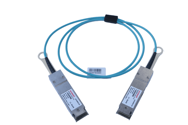
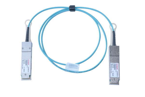
AAQPQP100Cxxx | 103.1Gbps | <70m | 0~70°C | Yes |
Note: xxx denotes the AOC length with unit meter.eg: 001 denotes 1m.


As shown in Figure 1, the transmitter path of the AOC (each end) contains a 4x25.78Gbps CAUI-4 electrical input with equalization (EQ) block, VCSEL laser drivers, VCSEL lasers and diagnostic monitor.
As shown in Figure 1, the receiver path of the AOC (each end) contains four PIN photodiodes, trans- impedance amplifiers (TIA) and 4x25.78G CAUI-4 compliant electrical output blocks.
The interface between QSFP28 module and ASIC/SerDes is shown in Figure 2. The high speed signal lines are internally AC-coupled and the electrical inputs are internally terminated to 100 ohms’ differential. All transmitter and receiver electrical channels are compliant to C2M CAUI-4 specifications per IEEE 802.3bm.
The control signal interface is compliant with QSFP28 MSA. The following pin is provided to control module or display the module status: ModSelL, ResetL, LPMode, IntL and ModPrsL. In addition, there is an industry standard two wire serial interface scaled for 3.3V LVTTL. The definition of control signal interface and the registers of the serial interface memory are defined in the Control Interface & Memory Map section.
Exposure to current surges and overvoltage events can cause immediate damage to the AOC module. Observe the precautions for normal operation of electrostatic discharge sensitive equipment; Attention shall also be paid to limiting AOC module exposure to conditions beyond those specified in the absolute maximum ratings.
Absolute Maximum Ratings
Parameter | Symbol | Min. | Typ. | Max. | Unit | Note |
Storage Temperature | Ts | -40 | - | 85 | ºC | |
Relative Humidity | RH | 5 | - | 85 | % | |
Power Supply Voltage | VCC | -0.5 | 3.3 | 3.6 | V |
Recommended Operating Conditions
Parameter | Symbol | Min. | Typ. | Max. | Unit | Note |
Case Operating Temperature | Tcase | 0 | - | 70 | ºC | Without air flow |
Power Supply Voltage | VCC | 3.135 | 3.3 | 3.465 | V | |
Power Supply Noise | ICC | - | 25 | mVpp | ||
Receiver Differential Data Output Load | 100 | ohm |
General Electrical Characteristics
Parameter | Symbol | Min. | Typical | Max. | Unit |
AOC Power Consumption (each end) | 2.5 | W | |||
AOC Power Supply Total Current (each end) | 758 | mA | |||
AC Coupling Internal Capacitor | 0.1 | μF |


High Speed Electrical Input Characteristics
Parameter | Test Point | Min. | Typical | Max. | Unit |
Signaling Rate per Lane | TP1 | 25.78125±100ppm | Gbps | ||
Differential Peak-Peak Input Voltage tolerance | TP1a | 900 | mV | ||
Differential Input Return Loss | TP1 | Equation(83E-5) | dB | ||
Common to Common Mode Input Return Loss | TP1 | Equation(83E-6) | dB | ||
Differential Termination Mismatch | TP1 | 10 | % | ||
Single-ended Voltage Tolerance Range | TP1a | -0.4 | 3.3 | V | |
DC Common-mode Output Voltage | TP1 | -350 | 2850 | mV | |
Module Stressed Input Test | TP1a | ||||
Eye Width | 0.46 | UI | |||
Applied Peak-Peak Sinusoidal Jitter | Table 88-13 | ||||
Eye Height | 95 | mV |
High Speed Electrical Output Characteristics
Parameter | Test Point | Min. | Typical | Max. | Unit |
Signaling Rate per Lane | TP4 | 25.78125±100ppm | Gbps | ||
AC Common-mode Output Voltage (RMS) | TP4 | 17.5 | mV | ||
Differential Peak-to-peak Output Voltage | TP4 | 900 | mV | ||
Eye Width | TP4 | 0.57 | UI | ||
Eye Height, Differential | TP4 | 228 | mV | ||
Vertical Eye Closure | TP4 | 5.5 | dB | ||
Differential Output Return Loss | TP4 | Equation(83E-2) | |||
Common to Differential Mode Conversion Return Loss | TP4 | Equation(83E-3) | |||
Differential Termination Mismatch | TP4 | 10 | % | ||
Transition Time (20% ~80%) | TP4 | 12 | ps | ||
DC Common Mode Voltage | TP4 | -350 | 2850 | mV |
The AAQPQP100CXXX is compatible with the ESD requirements described in the Regulatory Compliance Table. However, in the normal processing and operation of AOC, the following two types of situations need special attention.
Case I: Before inserting the AOC into the rack meeting the requirements of QSFP28 MSA, ESD preventive measures must be taken to protect the equipment. For example, the grounding wrist strap, workbench and
floor should be used wherever the AOC is handled.
Case II: After the AOC is installed, the electrostatic discharge outside the chassis of the host equipment shall be within the scope of system level ESD requirements. If the optical interface of the AOC is exposed outside the host equipment cabinet, the AOC may be subject to equipment system level ESD requirements.
Communication equipment with AOC is usually regulated by FCC in the United States and CENELEC EN55032 (CISPR 32) in Europe. The compliance of AAQPQP100CXXX with these standards is detailed in the regulatory compliance table. The metal shell and shielding design of AAQPQP100CXXX will help equipment designers minimize the equipment level EMI challenges they face.
AAQPQP100CXXX AOC meets UL certification requirements, its constituent materials have heat and corrosion resistance, and the plastic parts meet UL94V-0 requirements.
QSFP28 Electrical Pad Layout

Pin Assignment
Pin | Logic | Symbol | Description | Plug Sequence4 | Notes |
1 | GND | Ground | 1 | 1 | |
2 | CML-I | Tx2n | Transmitter Inverted Data Input | 3 | |
3 | CML-I | Tx2p | Transmitter Non-Inverted Data Input | 3 | |
4 | GND | Ground | 1 | 1 | |
5 | CML-I | Tx4n | Transmitter Inverted Data Input | 3 | |
6 | CML-I | Tx4p | Transmitter Non-Inverted Data Input | 3 | |
7 | GND | Ground | 1 | 1 | |
8 | LVTTL-I | ModSelL | Module Select | 3 | |
9 | LVTTL-I | ResetL | Module Reset | 3 | |
10 | VccRx | +3.3V Power Supply Receiver | 2 | 2 | |
11 | LVCMOS- I/O | SCL | 2-wire Serial Interface Clock | 3 | |
12 | LVCMOS- I/O | SDA | 2-wire Serial Interface Data | 3 | |
13 | GND | Ground | 1 | 1 | |
14 | CML-O | Rx3p | Receiver Non-Inverted Data Output | 3 | |
15 | CML-O | Rx3n | Receiver Inverted Data Output | 3 | |
16 | GND | Ground | 1 | 1 | |
17 | CML-O | Rx1p | Receiver Non-Inverted Data Output | 3 | |
18 | CML-O | Rx1n | Receiver Inverted Data Output | 3 | |
19 | GND | Ground | 1 | 1 | |
20 | GND | Ground | 1 | 1 | |
21 | CML-O | Rx2n | Receiver Inverted Data Output | 3 | |
22 | CML-O | Rx2p | Receiver Non-Inverted Data Output | 3 | |
23 | GND | Ground | 1 | 1 | |
24 | CML-O | Rx4n | Receiver Inverted Data Output | 3 | |
25 | CML-O | Rx4p | Receiver Non-Inverted Data Output | 3 | |
26 | GND | Ground | 1 | 1 | |
27 | LVTTL-O | ModPrsL | Module Present | 3 | |
28 | LVTTL-O | IntL | Interrupt | 3 | |
29 | VccTx | +3.3V Power Supply Transmitter | 2 | 2 | |
30 | Vcc1 | +3.3V Power Supply | 2 | 2 | |
31 | LVTTL-I | LPMode | Low Power Mode | 3 | |
32 | GND | Ground | 1 | 1 | |
33 | CML-I | Tx3p | Transmitter Non-Inverted Data Input | 3 | |
34 | CML-I | Tx3n | Transmitter Inverted Data Input | 3 | |
35 | GND | Ground | 1 | 1 | |
36 | CML-I | Tx1p | Transmitter Non-Inverted Data Input | 3 | |
37 | CML-I | Tx1n | Transmitter Inverted Data Input | 3 | |
38 | GND | Ground | 1 | 1 | |
1: GND is the symbol for signal and supply (power) common for the module. All are common within the module and all module voltages are referenced to this potential unless otherwise noted. Connect these directly to the host board signal- common ground plane. | |||||
2: VccRx, Vcc1 and VccTx are applied concurrently and maybe internally connected within the module in any combination. Vcc contacts in SFF-8662 and SFF-8672 each have a steady state current rating of 1A. | |||||

The host board should use a power supply filtering network equivalent to that shown in Figure 7.
Any voltage drop across a filter network on the host is counted against the host DC set point accuracy specification. Inductors with DC resistance of less than 0.1 ohm should be used in order to maintain the required voltage at the host edge card connector. It is recommended that the 22 μF capacitors each have an equivalent series resistance of 0.22 ohm.
The specification of the host power supply filtering network is beyond the scope of this specification, particularly because of the wide range of QSFP+ module Power Classes. Each power connection has a supply filter for reducing high frequency noise and ripple from host-to-module. During a hot-plug event, the filter network limits any voltage drop on the host supply so that neighboring modules sharing the same supply stay within their specified supply voltage limits.

Copyright 2022 ATI. All rights reserved.
Copyright 2022 ATI. All rights reserved.
Please fill the following information, we can better provide our services.